E-Beam and Optical Lithography
Electron Beam Lithography (EBL)
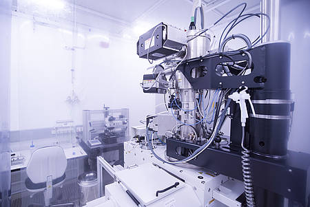
RAITH EBPG5150 EBL
The EBPG5150 electron beam lithography system is designed for high-resolution and high-accuracy patterning of devices on semiconductor wafers. Highly focused electron beams are used to draw circuit patterns on the nanometer scale onto semiconductor wafers coated with resists.
- High current density Thermal Field Emission gun for operation at 20-100 kV
- 155 mm platform
- Minimum feature size of less than 8 nm
- Rapid exposure with 50 or 100 MHz pattern generator
- Continuously variable large field size operation to 1 mm at all kVs
- GUI for ease of use operation for diverse “multi user environment”
- Thermal Field Emission (TFE) electron source
- Automatic dynamic off-axis focus, stigmation and distortion correction software
- Low noise 20-bit main field deflection
- Field size operation, variable up to 1mm by 1mm at all voltages
- Binocular microscope, X/Y stage and Laser Height sensor to pre-align wafers
- System control software suite “BEAMS” on fully integrated control PC.
User Support and Scientific Advice:
Salvatore Bagiante salvatore.bagiante@ist.ac.at
Juan Luis Aguilera juan.aguilera@ist.ac.at
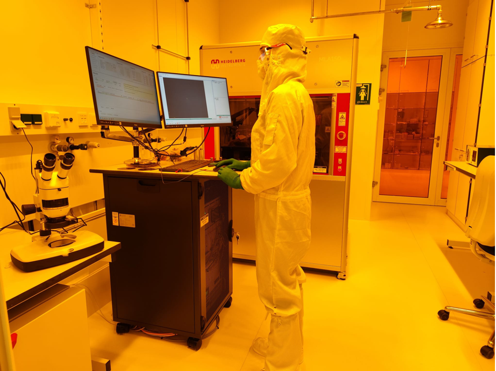
Maskless Lithography (MLA)
Heidelberg Instruments MLA 150
The MLA 150 is a high-speed, maskless direct-writing lithography system designed for accurate, and efficient patterning of photoresist-coated substrates. Its direct-write technology enhances performance and reduces operational costs by eliminating physical masks. A 375 nm exposure laser delivers sufficient energy to expose thick or less sensitive resists while maintaining excellent pattern accuracy, enabling the fabrication of features as small as 0.6 μm.
- Laser: 375 nm
- Feature size ≥ 0.6 μm
- Lines and spaces ≥ 0.8 μm
- Global 2nd layer alignment ≤ 0.5 μm
- Local 2nd layer alignment ≤ 0.25 μm
- Backside alignment ≤ 0.1 μm
- High aspect ratio mode for optimized sidewall profiles in thick resist
- Adjustable focus depth for improved pattern quality
- Wide range support of various substrate sizes
- Environmental chamber with controlled temperature and humidity
- Laminar airflow
User Support and Scientific Advice:
Carola Rando carola.rando@ist.ac.at
Juan Luis Aguilera juan.aguilera@ist.ac.at
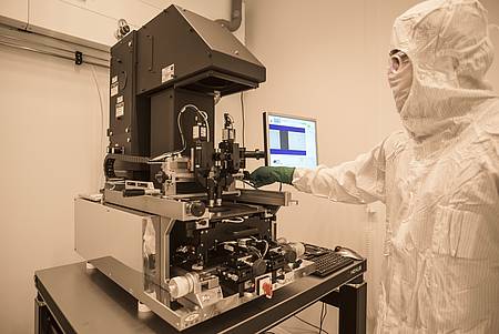
Mask Aligner
EVG 610 Mask Aligner
The EVG 610 is a semi-automated system that can handle small substrate pieces and wafers up to 200 mm. The tool supports lithography processes, such as vacuum-, soft-, hard- and proximity exposure mode.
- Supports back side lithography and bond alignment processes when configured with bottom side microscopes
- Sub-micron exposure gap repeatability in proximity exposure mode
- Unmatched exposure light uniformity at wafer level, down to ± 1.5% for small substrate applications
- Windows based user interface
User Support and Scientific Advice:
Lubuna Shafeek lubuna.shafeek@ist.ac.at
Carola Rando carola.rando@ist.ac.at
Nasima Afsharimani nafshari@ista.ac.at